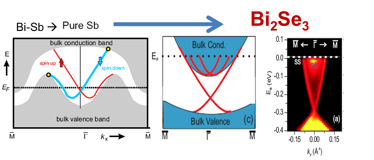
One of the central issues that has plagued the experimental progress with topological insulators is the presence of bulk doping or conductance in most naturally grown crystals. You can see this simply by looking at the ARPES plots below:
 (copyright Hasan lab, Princeton, see license in the beginning of the chapter)
What you see is that the Fermi-energy, which is the highest energy till which you can eject electrons in ARPES intersects the conduction band. This means that in the native state the conduction band of the electrons is occupied and the fermi level is not in the gap. In the figure above, the situation is worst for pure Antimony in the extreme left panel, which is really a semimetal with overlapping electron and hole bands. In this case, independent of fermi level position, the system would remain metallic. Moving from pure Sb to \(Bi_2 Se_3\) improves this somewhat, but still does not make this an insulator. Theoretically, we do expect pure \(Bi_2 Se_3\) to be an insulator - but in reality, the system typically have Se vacancies, which make it metallic.
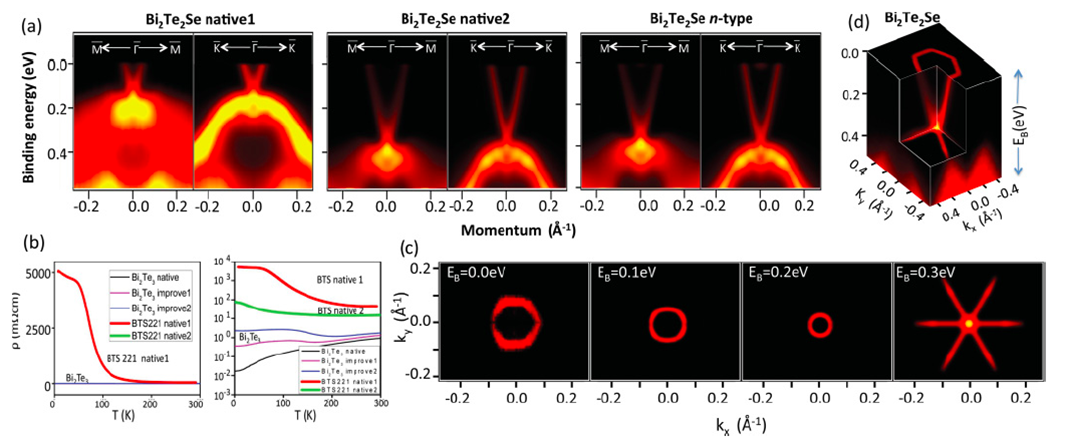
Being metallic really ruins a lot of interesting properties of the topological insulators. So a lot of effort is going in to fixing it up. Below, we see some of the results from these attempts:
 (copyright Hasan lab, Princeton, see license in the beginning of the chapter)
where various combinations of \(Bi\), \(Se\) and \(Te\) have been combined to drive the system insulating. By looking at the ARPES spectra, it should look convincing that by varying different conditions, the fermi level is indeed shifting in to the interior of the gap. The experimental tricks used to get this working range between changing the pressure of various elements in the growth condition to counter doping the surface etc. But the resistance results seem to be improving quite a bit.