
Unlike in the case of Majoranas, not much thinking is required to figure out the relevant signature of the quantum spin Hall effect. There is a pair of modes on each edge of the sample that is protected from backscattering. All the other modes are gapped or backscattered, so the edge states are the only ones to carry current. This current will not suffer from backscattering.
If we consider the simplest case, a sample with only two terminals, then Landauer’s formula together with the absence of backscattering gives the conductance \(G_0=2 e^2/h\).
When we move the Fermi level outside of the bulk gap, the bulk becomes conducting, and so the conductance increases.
We end up with this situation:
Here on the left we see a comparison between the conductances of a trivial (blue curve) and a topological (red curve) insulator as a function of chemical potential. The other two panels show the spectra of a quantum spin Hall insulator in the topological and trivial phases. As we expected, conductance is quantized when the chemical potential is inside the band gap of a topological system.
Let’s now see what can be measured experimentally.
(copyright JPS, see license in the beginning of the chapter)
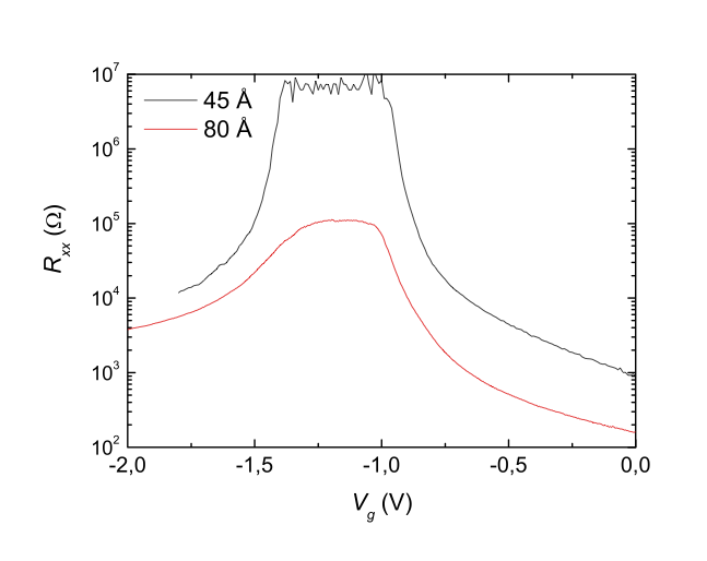
What you notice is that the maximum resistance for the 4.5 nm thick quantum well is much higher than for the 8 nm thick well. Given that theory predicts that the HgTe quantum wells described by Michael Wimmer in his video are topological when their thickness is between 6.3 nm and 12 nm, this measurement suggests that the lower resistance of the 8 nm thick well might be due to edge conductance. But even though it is the lower of the two, you might complain that the resistance of the 8 nm well is closer to \(100\) \(k\Omega\) than the predicted \(12\) \(k\Omega\) from the quantum of conductance.
The black curve here is the resistance of a trivial insulator, and the red one should be that of a topological one. The resistance of a trivial insulator becomes very high as expected, and there is a plateau-like feature in the topological regime.
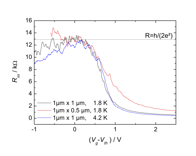
Fortunately, it was revealed in further experiments by the Wurzburg group, that by reducing the length of the sample from length \(L=20\) \(\mu m\) to \(L=1\) \(\mu m\), the conductance maximum rises to about \(12.9\) \(k\Omega\):
(copyright JPS, see license in the beginning of the chapter)
We see something different from what we expected: the average resistance value at the plateau is correct, but only within 10% precision, very different from the \(10^{-8}\) accuracy of the quantum Hall effect.
This difference most likely originates from backscattering. In the quantum Hall effect, backscattering is prohibited by the absence of modes going in the other direction. In the quantum spin Hall effect however, the protection is much weaker and is merely due to Kramers theorem.
The exact origin of the backscattering is hard to understand. It could be inelastic scattering that does not preserve energy, or it could also be some residual magnetic impurities, which break time reversal symmetry. In both cases, Kramers theorem does not hold. One of the papers that we suggest for review proposes an interesting theory for the origin of the backscattering, while another reports measurements of InAs/GaSb quantum well, where conductance seems much better quantized.
Regardless of the exact origin of backscattering, at any finite temperature, there is an inelastic scattering length \(l_\phi\) beyond which we do not expect any protection from scattering. When the edge length \(L\) is larger than \(l_\phi\), we expect the edge to turn into an incoherent conductor with resistance of \((e^2/h) l_\phi/L\).
In principle, this allows us to measure \(l_\phi\) for the quantum spin hall edges by looking at the length dependence of the conductance. Indeed, experiments find that small samples have conductance close to \(G_0\), while in large samples the conductance is suppressed.